Compare semiconductor diode and transistor. Semiconductor diodes and transistors, area of application
Semiconductor diode called a non-signal amplifying electronic element with one electron-hole junction and two leads from the anode and cathode.
Diodes are used in electronic circuits to convert the parameters of electrical signals (rectification, stabilization). Diodes differ in design ( point, planar) and according to the symbol on the diagrams (depending on the functional purpose).
Operating principle diode illustrates it volt-ampere characteristics, those. dependence of the current on the applied voltage, (Fig. 1), from which it is clear that the diode has one-way conductivity(passes current in the forward direction and practically does not pass it in the reverse direction).
The diode is connected in the forward direction when the positive pole of the current source is connected to the anode A, and the negative pole of the current source is connected to the cathode K. This corresponds to the characteristic branch in the first quadrant. A large forward current passes through the diode.
When connected to reverse direction (plus - to the cathode, minus - to the anode), the reverse current I OBR passing through the diode is very small (mkA).
In this case, the direct current, as can be seen from Fig. 1, depends significantly on temperature environment (increases with increasing temperature).
Rice. 1. Current-voltage characteristic of the diode.
Diode characteristics:
In addition to the considered current-voltage, the main characteristics of the diode include:
Maximum forward current I ETC ;
Temperature resistance t 0 max ;
Maximum reverse voltage U KP .
DC resistance R 0 = U ETC / I ETC ;
AC Resistance R i = Δ U ETC / Δ I ETC ;
Slope of the current-voltage characteristic S = Δ I ETC / Δ U ETC ;
Power loss at the anode P A = U ETC I ETC ;
Area of use of diodes: AC rectification; voltage stabilization; work in photovoltaic devices; work in microwave circuits, etc.
Transistors
Transistors – semiconductor devices with two r-p transitions allowing enhance electrical signal and usually having three terminals. Divided into two groups - bipolar and unipolar(field). Basic circuits for connecting a bipolar transistor - with a common base, with a common emitter and with a common collector. The type of switching circuit determines by what parameter the transistor amplifies the signal (voltage, current, etc.).
Bipolar transistor is a semiconductor device with a three-layer structure with alternating types of conductivity and two r-p transitions, allowing amplification of electrical signals and having three outputs. Distinguish direct (p-n-p) and reverse (n-p-n) transistors, the difference between which is polarity connecting power supplies.
The components of a transistor correspond to its layers and are named: emitter– charge emitter, base– base and collector– charge collector. Layers have
different conductivity: extreme (emitter and collector) - holep, and the base located between them is electronicn(Fig. 2).
Emitter Base Collector
Iuh ITo

EntranceExit
Rice. 2. Bipolar p- n- p transistor connected according to a common base circuit
Let's consider the principle of operation of a transistor. As can be seen in Fig. 2, the transistor has two junctions: p- n And n- p. First transition ( p- n) included in direct direction, i.e. minus k n-areas, and plus to R– areas - to the emitter. Therefore, direct current will flow through this junction. Second transition ( n- p) included in reverse direction, i.e. plus to base ( n- area), and minus to R– areas - to the collector. If you open the emitter (input) circuit, this junction, located under reverseU K when turned on, it will be practically closed.
If you close the emitter circuit (apply an input signal), through the first (open) p- n junction, a direct current will flow, formed by the injection of holes into the base. Since the thickness of the base is small, and the semiconductors from which the emitter and base are made are selected with different concentrations of the main carriers, i.e. the concentration of holes in the emitter is significantly higher than the concentration of electrons in the base, there will be so many holes in the base that only a small part of them will find in the base the electrons necessary for recombination. Therefore, incoming holes that have not recombined with electrons begin to move to those regions of the base that are adjacent to the collector. Positive holes approaching the collector junction, experiencing the action of a strong accelerating field from a powerful collector battery U K, pass into the collector and recombine with electrons coming into the collector from the negative pole of the battery. As a result, collector current will begin to flow through the collector junction I K, despite the fact that reverse voltage is applied to the junction. This collector current will be 90 - 95% of the emitter current (due to the small number of recombining holes remaining in the base). But the most important thing is that the magnitude of the collector current will depend on the magnitude of the emitter current and will change in proportion to its change. Indeed, the greater the current through the emitter junction, i.e., the more holes the emitter injects into the base, the greater the collector current, which depends on the number of these holes. This leads to a practically important conclusion:
By controlling the emitter current of the transistor, you can thereby control the collector current, and in this case an amplification effect takes place.
This property determined the area of use of transistors in amplifier circuits. So, for example, the considered circuit for connecting a transistor with a common base will give voltage and power gain input signal, since the output load resistance Rn with appropriate selection of battery voltage UTo may be significantly greater than the resistance at the amplifier input, i.e. R H >> R VX, and the input (emitter I E) and output (collector I TO) the currents are approximately equal. Hence the voltage and power supplied to the input U VX = I VX * R VX ; Pinput= I 2 input * Rinput less than the corresponding values of voltage and power at the output, i.e. in the load U = I TO * R N ; Pn = I K 2 * RN. There is no current gain in this case (since I E ~ = I TO).
More often, however, another transistor connection circuit is used - common emitter circuit, at which, in addition to power amplification, there is also current amplification. Connection diagram with common collector used when operating on a low-resistance load or from a high-resistance sensor. The gain of such a circuit in terms of current and power is several tens of units, and in terms of voltage - about one.
To correctly understand the principle of operation of transistor circuits, it is necessary to have a good understanding of the features of the operation of a transistor as an amplifier, which are as follows: unlike a vacuum tube, the transistor has a low input resistance in most switching circuits, as a result of which it is believed that the transistor is controlled by the input current, and not by the input current. tension; the low input resistance of transistor amplifiers leads to a noticeable consumption of power (current) from the source of amplified oscillations, therefore, in these amplifiers, the main importance is not voltage gain, but current or power gain; power gain k is determined by the ratio of the power allocated at the output of the amplifier in the payload to the power expended at the input impedance of the amplifier; The parameters and characteristics of the transistor are highly dependent on the temperature and the selected mode, which is a disadvantage.
Transistor characteristics:
Input, output and transient characteristics, fig. 3,

Rice. 3. Transistor characteristics: a – input, b – output, c – transition
Gain (transmission) in general terms, voltage, current, power
k=ΔΧ OUT /ΔΧ IN;ΔU OUT /ΔU IN;ΔI OUT /ΔI IN;ΔP OUT /ΔP IN.
Transistor AC input impedance
R = ΔU ВХ / ΔI ВХ.
Collector power loss
P K = U K * I K .
Advantages of transistors: small dimensions, high sensitivity, inertia-free; durability; flaws: significant influence of external factors (temperature, e/m fields, radioactive radiation, etc.).
Area of use transistors: Wired and radio communications; TV; radar; radio navigation; automation and telemechanics; Computer Engineering; measuring technology; amplifier circuits; memory chips for digital devices, etc.
Prepared
Student of class 10 "A"
School No. 610
Ivchin Alexey
Abstract on the topic:
“Semiconductor diodes and transistors, their areas of application”
1. Semiconductors: theory and properties
2. Basic semiconductor devices (Structure and application)
3. Types of semiconductor devices
4. Production
5. Scope of application
1. Semiconductors: theory and properties
First you need to get acquainted with the conduction mechanism in semiconductors. And to do this, you need to understand the nature of the bonds that hold the atoms of a semiconductor crystal near each other. For example, consider a silicon crystal.
Silicon is a tetravalent element. This means that in the external
The shell of an atom has four electrons that are relatively weakly bound to the nucleus. The number of nearest neighbors of each silicon atom is also four. The interaction of a pair of neighboring atoms is carried out using a polyelectronic bond, called a covalent bond. In the formation of this bond, one valence electron from each atom participates, which are split off from the atoms (collectivized by the crystal) and during their movement spend most of the time in the space between neighboring atoms. Their negative charge holds the positive silicon ions near each other. Each atom forms four bonds with its neighbors, and any valence electron can move along one of them. Having reached a neighboring atom, it can move on to the next one, and then further along the entire crystal.
Valence electrons belong to the entire crystal. The pair-electron bonds of silicon are quite strong and do not break at low temperatures. Therefore, silicon at low temperatures does not conduct electric current. The valence electrons involved in the bonding of atoms are firmly attached to the crystal lattice, and the external electric field does not have a noticeable effect on their movement.
Electronic conductivity.
When silicon is heated, the kinetic energy of the particles increases and individual bonds break. Some electrons leave their orbits and become free, like electrons in a metal. In an electric field, they move between lattice nodes, forming an electric current.
The conductivity of semiconductors due to the presence of free electrons in metals is called electronic conductivity. As the temperature increases, the number of broken bonds, and therefore free electrons, increases. When heated from 300 to 700 K, the number of free charge carriers increases from 10.17 to 10.24 1/m.3. This leads to a decrease in resistance.
Hole conductivity.
When a bond is broken, a vacant site with a missing electron is formed.
It's called a hole. The hole has an excess positive charge compared to other, normal bonds. The position of the hole in the crystal is not constant. The following process occurs continuously. One of the electrons that ensures the connection of atoms jumps to the place of the formed holes and restores the pair-electron bond here. and where this electron jumped from, a new hole is formed. Thus, the hole can move throughout the crystal.
If the electric field strength in the sample is zero, then the movement of holes, equivalent to the movement of positive charges, occurs randomly and therefore does not create an electric current. In the presence of an electric field, an ordered movement of holes occurs, and thus, the electric current associated with the movement of holes is added to the electric current of free electrons. The direction of movement of holes is opposite to the direction of movement of electrons.
So, in semiconductors there are two types of charge carriers: electrons and holes. Therefore, semiconductors have not only electronic but also hole conductivity. Conductivity under these conditions is called the intrinsic conductivity of semiconductors. The intrinsic conductivity of semiconductors is usually low, since the number of free electrons is small, for example, in germanium at room temperature ne = 3 per 10 in 23 cm in –3. At the same time, the number of germanium atoms in 1 cubic cm is about 10 in 23. Thus, the number of free electrons is approximately one ten-billionth of the total number of atoms.
An essential feature of semiconductors is that in the presence of impurities, along with their own conductivity, an additional one appears - impurity conductivity. By changing the impurity concentration, you can significantly change the number of charge carriers of one or another sign. Thanks to this, it is possible to create semiconductors with a predominant concentration of either negatively or positively charged carriers. This feature of semiconductors opens up wide possibilities for practical applications.
Donor impurities.
It turns out that in the presence of impurities, for example arsenic atoms, even at very low concentrations, the number of free electrons increases many times. This happens for the following reason. Arsenic atoms have five valence electrons, four of which are involved in creating a covalent bond between this atom and surrounding atoms, for example, with silicon atoms. The fifth valence electron appears to be weakly bound to the atom. It easily leaves the arsenic atom and becomes free. The concentration of free electrons increases significantly, and becomes a thousand times greater than the concentration of free electrons in a pure semiconductor. Impurities that easily donate electrons are called donor impurities, and such semiconductors are n-type semiconductors. In an n-type semiconductor, electrons are the majority charge carriers and holes are the minority charge carriers.
Acceptor impurities.
If indium, whose atoms are trivalent, is used as an impurity, then the nature of the conductivity of the semiconductor changes. Now, to form normal pair-electronic bonds with its neighbors, the indium atom lacks an electron. As a result, a hole is formed. The number of holes in the crystal is equal to the number of impurity atoms. Impurities of this kind are called acceptor impurities. In the presence of an electric field, holes move around the field and hole conduction occurs. Semiconductors with a predominance of hole conductivity over electron conductivity are called p-type semiconductors (from the word positiv - positive).
2. Basic semiconductor devices (Structure and application)
There are two basic semiconductor devices: the diode and the transistor.
Diode.
Nowadays, diodes are increasingly used in semiconductors to rectify electric current in radio circuits, along with two-electrode lamps, since they have a number of advantages. In a vacuum tube, charge carriers electrons are created by heating the cathode. In a p-n junction, charge carriers are formed when an acceptor or donor impurity is introduced into the crystal. Thus, there is no need for an energy source to obtain charge carriers. In complex circuits, the energy savings resulting from this turn out to be very significant. In addition, semiconductor rectifiers with the same values of rectified current are more miniature than tube rectifiers.
The current-voltage characteristic for forward and reverse connections is shown in Figure 2.
They replaced lamps and are very widely used in technology, mainly for rectifiers; diodes have also found application in various devices.
Transistor.
Let's consider one type of transistor made of germanium or silicon with donor and acceptor impurities introduced into them. The distribution of impurities is such that a very thin (on the order of several micrometers) layer of n-type semiconductor is created between two layers of p-type semiconductor Fig. 3.
This thin layer is called the base or base. Two p-n junctions are formed in the crystal, the direct directions of which are opposite. Three terminals from areas with different types of conductivity allow you to include a transistor in the circuit shown in Figure 3. With this connection, the left p-n junction is direct and separates the base from the area with p-type conductivity, called the emitter. If there were no right p –n
-transition, in the emitter-base circuit there would be a current depending on the voltage of the sources (battery B1 and the alternating voltage source) and the resistance of the circuit, including the low resistance of the direct emitter-base junction. Battery B2 is connected so that the right pn junction in the circuit (see Fig. 3) is reverse. It separates the base from the right p-type region called the collector. If there were no left pn junction, the current strength in the collector circuit would be close to zero. Since the reverse junction resistance is very high. When a current exists in the left p-n junction, a current appears in the collector circuit, and the current strength in the collector is only slightly less than the current strength in the emitter. When a voltage is created between the emitter and the base, the main carriers of the p-type semiconductor - holes penetrate the base, GDR they are already the main carriers. Since the thickness of the base is very small and the number of main carriers (electrons) in it is small, the holes that get into it almost do not combine (do not recombine) with the electrons of the base and penetrate into the collector due to diffusion. The right pn junction is closed to the main charge carriers of the base - electrons, but not to holes. In the collector, holes are carried away by the electric field and complete the circuit.
The strength of the current branching into the emitter circuit from the base is very small, since the cross-sectional area of the base in the horizontal (see Fig. 3) plane is much smaller than the cross-section in the vertical plane. The current strength in the collector, almost equal to the current strength in the emitter, changes along with the current in the emitter.
The resistance of the resistor R has little effect on the current in the collector, and this resistance can be made quite large. By controlling the emitter current using an alternating voltage source connected to its circuit, we obtain a synchronous change in the voltage across the resistor. If the resistance of the resistor is large, the change in voltage across it can be tens of thousands of times greater than the change in the signal in the emitter circuit. This means an increase in voltage. Therefore, using a load R, it is possible to obtain electrical signals whose power is many times greater than the power entering the emitter circuit. They replace vacuum tubes and are widely used in technology.
3. Types of semiconductor devices.
In addition to planar diodes (Fig. 8) and transistors, there are also point diodes (Fig. 4). Point transistors (structure see in the figure) are molded before use, i.e. pass a current of a certain magnitude, as a result of which an area with hole conductivity is formed under the tip of the wire. Transistors come in p-n-p and n-p-n types. Designation and general view in Figure 5.
There are photo- and thermistors and varistors as shown in the figure. Planar diodes include selenium rectifiers. The basis of such a diode is a steel washer, coated on one side with a layer of selenium, which is a semiconductor with hole conductivity (see Fig. 7). The surface of selenium is coated with a cadmium alloy, resulting in the formation of a film with electronic conductivity, as a result of which a rectifying current transition is formed. The larger the area, the greater the rectifying current.
4. Production
The diode manufacturing technology is as follows. A piece of indium is melted on the surface of a square plate with an area of 2-4 cm2 and a thickness of several fractions of a millimeter, cut from a semiconductor crystal with electronic conductivity. Indium is firmly alloyed with the plate. In this case, indium atoms penetrate
(diffuse) into the thickness of the plate, forming in it a region with a predominance of hole conductivity, Fig. 6. This results in a semiconductor device with two regions of different types of conductivity, and a p-n junction between them. The thinner the semiconductor wafer. the lower the resistance of the diode in the forward direction, the greater the current corrected by the diode. The diode contacts are an indium droplet and a metal disk or rod with lead conductors.
After assembling the transistor, it is mounted in the housing and the electrical connection is connected. leads to the contact plates of the crystal and the lead of the package and seal the package.
5. Scope of application
Diodes are highly reliable, but the limit of their use is from –70 to 125 C. Because a point diode has a very small contact area, so the currents that such diodes can deliver are no more than 10-15 mA. And they are used mainly for modulating high-frequency oscillations and for measuring instruments. For any diode, there are certain maximum permissible limits of forward and reverse current, depending on the forward and reverse voltage and determining its rectifying and strength properties.
Transistors, like diodes, are sensitive to temperature and overload and penetrating radiation. Transistors, unlike radio tubes, burn out due to improper connection.
-----------------------
Figure 2
Picture 1
Figure 3
Figure 4
Figure 5
Figure 4
SEMICONDUCTOR DIODES
Semiconductor diodes are semiconductor devices with one electrical junction and two terminals. They are used to rectify alternating current, detect alternating oscillations, convert microwave oscillations into intermediate frequency oscillations, stabilize voltage in direct current circuits, etc. According to their purpose, semiconductor diodes are divided into rectifier diodes, high-frequency diodes, varicaps, zener diodes, etc.
Rectifier diodes. Rectifier semiconductor diodes are designed to convert alternating current into direct current.
The basis of modern rectifier diodes is an electron-hole junction (EDJ), which is obtained by fusion or diffusion. The material used is germanium or silicon.
To obtain large values of rectified currents in rectifying diodes, EAFs with a large area are used, since for normal operation of the diode, the current density through the junction should not exceed 1-2 A/mm 2.
Such diodes are called planar. The design of a low-power planar semiconductor diode is shown in Fig. 2.1, a. To improve heat dissipation in medium-sized diodes And of high power, a screw is welded to their body, with which the diodes are attached to a special radiator or chassis (Fig. 2.1, b).
The main characteristic of a rectifier diode is its current-voltage characteristic (volt-ampere characteristic). The type of current-voltage characteristic depends on the semiconductor material and temperature (Fig. 2.2, a and b).

The main parameters of rectifying semiconductor diodes are:
constant forward voltage U np at a given forward current;
the maximum permissible reverse voltage U o 6 p max at which the diode can still operate normally for a long time;
constant reverse current flowing through the diode at a reverse voltage equal to U o 6 p max ;
average rectified current, which can pass through the diode for a long time at an acceptable temperature of its heating;
maximum permissible power dissipated by the diode, at which ensures the specified reliability of the diode.
According to the maximum permissible value of the average rectified current, diodes are divided into low-power (), medium-power ( ![]() ) and high power (). High power rectifier diodes are called power diodes.
) and high power (). High power rectifier diodes are called power diodes.
Low-power rectifier elements, which are rectifier semiconductor diodes connected in series, are called rectifier columns. Rectifier units are also produced in which rectifier diodes are connected according to a certain (for example, bridge) circuit.
Rectifier semiconductor diodes are capable of operating at frequencies of 50... 10 5 Hz (power diodes - at frequencies of 50 Hz), i.e. they are low-frequency.
High frequency diodes. High-frequency diodes include semiconductor diodes capable of operating at frequencies up to 300 MHz. Diodes operating at frequencies above 300 MHz are called ultra-high frequency (microwave).
As the frequency increases, the shunting of the differential resistance of the reverse-biased EHP by the charging capacitance increases. This leads to a decrease in reverse resistance and a deterioration in the rectifying properties of the diode. Since the value of the charging capacity is proportional to the area of the EAF, to reduce it it is necessary to reduce the area of the EAF.
Microalloy diodes have a small junction area, but they... The disadvantage is the accumulation of minority charge carriers in the base, which are injected into it when the diode is directly turned on. This limits the performance (frequency range) of microalloy diodes.
Point diodes capable of operating in the microwave range have better performance and, therefore, higher frequencies. In their design, a metal spring with a diameter of about 0.1 mm is pressed with its tip against a semiconductor crystal. The spring material is selected so that the work function of electrons from it is greater than from the semiconductor. In this case, a blocking layer is formed at the metal-semiconductor interface, called the Schottky barrier - named after the German scientist who studied this phenomenon. Diodes whose operation is based on the properties of the Schottky barrier are called Schottky diodes. In them, the electric current is carried by the majority charge carriers, as a result of which there are no phenomena of injection and accumulation of minority charge carriers.
High-frequency and microwave diodes are used for rectifying high-frequency oscillations (rectifier), detection (detector), power level control (switching), frequency multiplication (multiplying) and other nonlinear transformations of electrical signals.
Varicaps. Varicaps are semiconductor diodes whose action is based on the dependence of capacitance on reverse voltage. Varicaps are used as an element with electrically controlled capacitance.
The nature of the dependence is shown in Fig. 2.3, a. This dependence is called the capacitance-voltage characteristic of a varicap. Main parameters

varicaps are:
rated capacitance measured at a given reverse voltage;
capacitance overlap coefficient Kc, determined by the ratio of the varicap capacitances at two values of reverse voltage;
maximum permissible reverse voltage;
quality factor Q B defined as the ratio of the varicap reactance to the loss resistance.
Semiconductor zener diodes. A semiconductor zener diode is a semiconductor diode, the voltage across which is maintained with a certain accuracy when the current passing through it changes in a given range. It is designed to stabilize voltage in DC circuits.
The current-voltage characteristic of the zener diode is shown in Fig. 2.4, a, and the symbol is in Fig. 2.4, b.

If an EDP is created on both sides of a silicon wafer, you will get a zener diode with a symmetrical current-voltage characteristic - a symmetrical zener diode (Fig. 2.4, c).
The working section of the zener diode is the section of electrical breakdown. When the current flowing through the zener diode changes from value to value. the voltage across it differs little from the value. The use of zener diodes is based on this property.
The principle of operation of a voltage stabilizer on a silicon zener diode (Fig. 2.4, d) is that when the voltage U VX changes, the current flowing through the zener diode changes, and the voltage on the zener diode and the load R connected in parallel to it practically does not change.
The main parameters of silicon zener diodes are:
stabilization voltage U st;
minimum and maximum stabilization currents;
maximum permissible power dissipation
differential resistance in the stabilization section ![]() ;
;
temperature coefficient of voltage in the stabilization section

In modern zener diodes, the stabilization voltage ranges from 1 to 1000 V with stabilization currents from 1 mA to 2 A. To stabilize voltages less than 1 V, the direct branch of the I-V characteristic of a silicon diode, called a stabistor, is used. For zener diodes B. By connecting zener diodes (or stabistors) in series, you can obtain any required stabilization voltage.
The differential resistance in the stabilization section is approximately constant and for most zener diodes it is 0.5...200 Ohm. The temperature coefficient of voltage can be positive (for zener diodes with ) and negative (for zener diodes with U CT< 6 В) и для большинства стабилитронов находится в пределах (- 0,5... + 0,2) %/°С.
BIPOLAR TRANSISTORS
A bipolar transistor (BT) or simply a transistor is a semiconductor device with two interacting EDPs and three or more terminals, the amplifying properties of which are determined by the phenomena of injection and extraction of minority charge carriers.
Electron-hole junctions are formed between three regions of a semiconductor with different types of electrical conductivity. In accordance with the order of alternation of p- and n-regions, BTs are divided into transistors of the p-p-p type and transistors of the p-p-p type (Fig. 2.5).

The middle region of the transistor is called the base, one extreme region is the emitter (E), and the other is the collector (K). Usually the concentration of impurities in the emitter is greater than in the collector. In a p-p-p type BT, the base has p-type electrical conductivity, and the emitter and collector are n-type.
The EDP formed between the emitter and the base is called emitter, and between the base and collector - collector.
Transistor operating modes. Depending on the method of connecting the emitter and collector EDP to power sources, the bipolar transistor can operate in one of four modes: cutoff, saturation, active and inverse.
The emitter and collector EAFs in the cutoff mode (Fig. 2.6, a) are shifted in the reverse direction, and in the saturation mode (Fig. 2.6, 6) - in the forward direction. The collector current in these modes is practically independent of the emitter voltage and current.

Cutoff and saturation modes are used when operating BT in pulsed and key devices.
When the transistor operates in the active mode, its emitter junction is shifted in the forward direction, and the collector junction in the opposite direction (Fig. 2.6, c).
Under the influence of direct voltage 11e, a current flows in the emitter circuit, creating collector and base currents, so
The collector current contains two components: controlled, proportional to the emitter current, and uncontrolled, created by the drift of minority carriers through the reverse biased collector junction. The proportionality factor is called the static transfer coefficient of the emitter current. For most modern BTs ![]() and more.
and more.
The base current includes a recombination component, caused by electrons entering the base to compensate for the positive charge of holes recombining in the base, and an uncontrolled component of the collector current, so that ![]()
When using a BT as an amplifying element, one of the terminals must be common to the input and output circuits. In the diagram shown in Fig. 2.6, c, the common electrode is the base. Such a BT connection circuit is called a common base (CB) circuit and is usually depicted as shown in Fig. 2.7, a. In addition to the OB circuit, circuits with a common emitter (CE) and a common collector (CC) are also used in practice.

In the OE circuit (Fig. 2.7, b), the relationship between the output and input currents is determined by the equation
The coefficient is called the static base current transfer coefficient. It is related to the ratio
At ![]() the values are in the range 19...99.
the values are in the range 19...99.
The component represents the reverse (uncontrolled) collector current in the OE circuit. This current is connected to the reverse current in the circuit
About the ratio
From relation (2.4) it follows that the reverse collector current in the OE circuit is much greater than in the OB circuit. This means that a change in temperature in the OE circuit has a greater effect on the change in currents (and therefore on changes in static characteristics and parameters) than in the OB circuit. This is one of the disadvantages of including BT under the OE scheme.
When you turn on the BT according to the OK scheme. (Fig. 2.7, c) the connection between the output and input currents is determined by the relation
From a comparison of expressions (2.2) and (2.5) it follows that the dependencies between the input and output currents of the BT in the OE and OK circuits are approximately the same. This allows you to use the same characteristics and parameters for calculating OE and OK circuits.
The inverse mode differs from the active mode by the opposite polarity of the voltages applied to the emitter and collector of the EAF.
Static characteristics. Static characteristics express complex relationships between currents and voltages
the electrodes of the transistor and depend on the method of its connection.
 |
In Fig. 2.8, a shows a family of input characteristics of a BT of the n - p - n type, connected according to the OE circuit, which express the dependence at . When the input characteristic is
direct branch of the current-voltage characteristic of the emitter EDP. When the collector voltage is positive, the input characteristic shifts to the right.
The output characteristics (Fig. 2.8, b) reflect the dependence at . The steep part of the characteristics corresponds to the saturation mode, and the flat part corresponds to the active mode. The relationship between the collector and base currents in a flat section is determined by expression (2.2).
Small signal parameters of static mode. When a transistor operates in amplification mode, its properties are determined by small-signal parameters, for which the transistor can be considered a linear element. In practice, small-signal hybrid or h-parameters are most widely used. Currents and voltages at small amplitudes of variable components in the system of h-parameters are related by the following relationships:
![]()
![]() - input resistance;
- input resistance;
 - voltage feedback coefficient
![]() - direct current transfer coefficient;
- direct current transfer coefficient;
![]() - output conductivity.
- output conductivity.
Parameters and are measured in the short circuit mode of the output circuit, and parameters and are measured in the idle mode of the input circuit. These modes are easy to implement. The values of h-parameters depend on the method of switching on the transistor and at low frequencies can be determined from static characteristics. In this case, the amplitudes of small currents and voltages are replaced by increments. So, for example, when a transistor is turned on according to a circuit with an OE, the formulas for parameters and , determined from the input characteristics at point A (Fig. 2.8, a), are written in the form:

Parameters and are determined by the output (Fig. 2.8, b) characteristics using the formulas:

The -parameters are determined similarly when the transistor is turned on according to the circuit with OB.
Small-signal parameters are accordingly called transfer coefficients of the emitter current and base current. They characterize the amplification properties of the transistor in terms of current for alternating signals, and their values depend on the operating mode of the transistor and on the frequency of the amplified signals. Thus, with increasing frequency, the modulus of the base current transfer coefficient decreases
The frequency at which it decreases by a factor of its value at a low frequency is called the limiting frequency of base current transmission and is designated . The frequency at which it decreases to 1 is called the BT cut-off frequency and is designated . Based on the value of the cutoff frequency, transistors are divided into low-frequency, mid-frequency, high-frequency and ultra-high-frequency.
THYRISTORS
A thyristor is a semiconductor device with two stable states, which has three or more transitions and can switch from a closed state to an open state and vice versa.
Thyristors with two terminals are called diodes or dinistors, and those with three terminals are called triodes or thyristors.
Dinistors. The dinistor structure consists of four semiconductor regions with alternating types of electrical conductivity ![]() , between which three EDPs are formed. The extreme EDPs are emitter, and the middle one is collector. The region is called the emitter or anode, the region is called the cathode.
, between which three EDPs are formed. The extreme EDPs are emitter, and the middle one is collector. The region is called the emitter or anode, the region is called the cathode.
Connecting the anode of the dinistor to the positive pole of an external source, and the cathode to the negative, corresponds to the direct connection of the dinistor. When the polarity of the source voltage is reversed, reverse switching occurs.
When connected directly, the dinistor can be represented as a combination of two transistors p - n - p and n - p - n (Fig. 2.9, a) with emitter current transfer coefficients and .

The current flowing through the dinistor contains the hole injection component of the transistor, the electronic injection component of the transistor and the reverse current of the collector junction, i.e.
![]()
![]()
For now, the dinistor is closed. At ![]() processes develop in the dinistor, leading to an avalanche-like increase in the injection current components and switching the collector junction in the forward direction. In this case, the resistance of the dinistor decreases sharply and the voltage drop across it does not exceed 1-2 V. The rest of the source voltage drops across the limiting resistor (Fig. 2.9, b).
processes develop in the dinistor, leading to an avalanche-like increase in the injection current components and switching the collector junction in the forward direction. In this case, the resistance of the dinistor decreases sharply and the voltage drop across it does not exceed 1-2 V. The rest of the source voltage drops across the limiting resistor (Fig. 2.9, b).
When the dinistor is turned back on, a small reverse current flows through it.
SCR. A thyristor differs from a dinistor in the presence of an additional control output from the base area (Fig. 2.10, a). The conclusion can be made from any base. A source connected to this pin creates

control current, which adds up to the main current. As a result, the thyristor switches from a closed state to an open state at a lower value of U a (Fig. 2.10, b).
In five-layer structures ![]() by appropriately performing the extreme regions, you can obtain a symmetrical current-voltage characteristic (Fig. 2.10, c). Such a thyristor is called symmetrical. It can be diode (diac) or triode (triac).
by appropriately performing the extreme regions, you can obtain a symmetrical current-voltage characteristic (Fig. 2.10, c). Such a thyristor is called symmetrical. It can be diode (diac) or triode (triac).
The thyristor is turned off by reducing (or interrupting) the anode current or changing the polarity of the anode voltage.
The thyristors considered are called non-lockable. There are also turn-off thyristors, which can be switched from open to closed by changing the control electrode current. They differ from non-lockable ones in design.
Thyristor parameters. The main parameters of thyristors are:
switch-on voltage;
unlocking control current;
switch-off current ;
residual stress U np ;
switching time t on;
shutdown time;
delay time t 3 ;
maximum rates of rise of forward voltage (du/dt) max and forward current (di/dl) max.
Thyristors are widely used in controlled rectifiers, DC-AC converters (inverters), voltage stabilizers,

as contactless switches, in electric drives, automation devices, telemechanics, computer technology, etc.
Symbols of thyristors are shown in Fig. 2.11.
FIELD TRANSISTORS
A field-effect transistor (FET) is a semiconductor device whose amplifying properties are determined by the flow of main charge carriers of the same sign flowing through a conducting channel and which is controlled by an electric field.
The control electrode, isolated from the channel, is called a gate. Based on the method of gate insulation, field-effect transistors are divided into three types:
1) with a control p-n junction, or with a p-t gate;
2) with a metal semiconductor gate, or with a Schottky gate;
3) with an insulated shutter.
Field effect transistors with p- n - shutter In a field-effect transistor with a p-n gate (Fig. 2.12), the n-type channel is isolated from the substrate and the p-n gate

moves, which, due to the fulfillment of the condition, are formed mainly in the channel. When the thickness of the channel is greatest, and its resistance is minimal. If a negative voltage is applied to the gate relative to the source, then the p-n junctions will expand, the thickness of the channel will decrease, and its resistance will increase. Therefore, if a voltage source is connected between the source and drain, then the current Ic flowing through the channel can be controlled by changing the resistance of the channel using the voltage applied to the gate. The operation of a PT with a p-n gate is based on this principle.
The main static characteristics of a PT with a p-n gate are the transfer (drain-gate) and output (drain) characteristics (Fig. 2.13).
The gate voltage at which the channel is completely blocked and the drain current is reduced to tenths of a microampere is called the cutoff voltage and is designated .
The drain current at U 3I = 0 is called the initial drain current.
The output characteristics contain steep, or ohmic, and flat regions. The flat region is also called the saturation region or the channel overlap region.

The drain current flowing through the channel creates a voltage drop across its distributed resistance, which increases the channel-gate and channel-substrate reverse voltages, which leads to a decrease in the channel thickness. The reverse voltages reach their greatest value at the boundary with the drain, and in this area the narrowing of the channel is maximum (Fig. 2.12). At a certain voltage value, both p-n junctions close in the drain region and the channel overlaps. This drain voltage is called the flashover voltage or saturation voltage (). When a reverse voltage is applied to the gate, an additional narrowing of the channel occurs, and its blocking occurs at a lower voltage value.
Field effect transistors with Schottky gate. IN PT with a Schottky gate, the channel resistance is controlled by changing, under the action of the gate voltage, the thickness of the rectifying junction formed at the interface between the metal and the semiconductor. Compared to a p-n junction, a rectifying metal-semiconductor junction allows one to significantly reduce the channel length: up to 0.5...1 µm. At the same time, the dimensions of the entire structure of the FET are significantly reduced, as a result of which FETs with a Schottky barrier are able to operate at higher frequencies - up to 50...80 GHz.
Field-effect transistors with insulated gate. These transistors have a metal-dielectric-semiconductor structure and are briefly called MOS transistors. If silicon oxide is used as a dielectric, then they are also called MOS transistors.
There are two types of MOS transistors: with induced and with built-in channels.
In MOS transistors with an induced p-type channel (Fig. 2.14), the p-type drain and source regions form two counter-current regions with the n-region of the substrate

EAFs are turned on, and when a source of any polarity is connected to them, there will be no current in the circuit. If a negative voltage is applied to the gate relative to the source and substrate, then at a sufficient value of this voltage in the near-surface layer of the semiconductor located under the gate, an inversion of the type of electrical conductivity will occur and the p-regions of the drain and source will be connected by a p-type channel. This gate voltage is called the threshold voltage and is designated . As the negative gate voltage increases, the penetration depth of the inversion layer into the semiconductor increases, which corresponds to an increase in the thickness of the channel and a decrease in its resistance.
The transfer and output characteristics of an MOS transistor with an induced p-type channel are presented in Fig. 2.15. The voltage drop across the channel resistance reduces the voltage between the gate

and channel and channel thickness. The greatest narrowing of the channel will be at the drain, where the voltage is lowest ![]() .
.
In MOS transistors with a built-in channel between the drain and source regions, a thin near-surface layer (channel) with the same type of electrical conductivity as the drain and source is created already at the manufacturing stage. Therefore, in such transistors, the drain current, called the initial current, flows at .
The static output and transfer characteristics of a MOS transistor with a built-in p-type channel are shown in Fig. 2.16.

Differential parameters of PT. In addition to the parameters discussed above, the properties of the PT are characterized by differential parameters: the slope of the transfer characteristic, or the slope of the PT; differential resistance and static gain.
The slope of the PT at characterizes the amplification properties of the transistor and for low-power transistors is usually several mA/V.
The differential resistance at represents the resistance of the DC channel to alternating current.
The slope of the PT can be determined by the static output or transfer characteristics (Fig. 2.16) based on the expression
and the differential resistance - according to the output characteristics in accordance with the expression
Static gain ![]() at is usually calculated using the formula.
at is usually calculated using the formula.
Conventional graphic symbols of field-effect transistors are shown in Fig. 2.17.

Field-effect transistors are used in amplifiers with high input resistance, switch and logic devices, as well as in controlled attenuators as an element whose resistance changes under the influence of control voltage.
Related information.
1. Semiconductors: theory and properties
2. Basic semiconductor devices (Structure and application)
3. Types of semiconductor devices
4. Production
5. Scope of application
1. Semiconductors: theory and properties
First you need to get acquainted with the conduction mechanism in semiconductors. And to do this, you need to understand the nature of the bonds that hold the atoms of a semiconductor crystal near each other. For example, consider a silicon crystal.
Silicon is a tetravalent element. This means that in the external
the shell of an atom has four electrons, relatively weakly bound
with a core. The number of nearest neighbors of each silicon atom is also equal to
four. The interaction of a pair of neighboring atoms is carried out using
paionoelectronic bond called covalent bond. In education
this bond from each atom involves one valence electron, co-
which are split off from atoms (collectivized by the crystal) and when
in their movement they spend most of their time in the space between
neighboring atoms. Their negative charge holds the positive silicon ions near each other. Each atom forms four bonds with its neighbors,
and any valence electron can move along one of them. Having reached a neighboring atom, it can move on to the next one, and then further along the entire crystal.
Valence electrons belong to the entire crystal. The pair-electron bonds of silicon are quite strong and do not break at low temperatures. Therefore, silicon at low temperatures does not conduct electric current. The valence electrons involved in the bonding of atoms are firmly attached to the crystal lattice, and the external electric field does not have a noticeable effect on their movement.
Electronic conductivity.
When silicon is heated, the kinetic energy of the particles increases, and
individual connections are broken. Some electrons leave their orbits and become free, like electrons in a metal. In an electric field, they move between lattice nodes, forming an electric current.
The conductivity of semiconductors due to the presence of free metals
electrons electrons is called electron conductivity. As the temperature increases, the number of broken bonds, and therefore free electrons, increases. When heated from 300 to 700 K, the number of free charge carriers increases from 10.17 to 10.24 1/m.3. This leads to a decrease in resistance.
Hole conductivity.
When a bond is broken, a vacant site with a missing electron is formed.
It's called a hole. The hole has an excess positive charge compared to other, normal bonds. The position of the hole in the crystal is not constant. The following process occurs continuously. One
from the electrons that ensure the connection of atoms, jumps to the place of exchange
formed holes and restores the pair-electronic bond here.
and where this electron jumped from, a new hole is formed. So
Thus, the hole can move throughout the crystal.
If the electric field strength in the sample is zero, then the movement of holes, equivalent to the movement of positive charges, occurs randomly and therefore does not create an electric current. In the presence of an electric field, an ordered movement of holes occurs, and thus, the electric current associated with the movement of holes is added to the electric current of free electrons. The direction of movement of holes is opposite to the direction of movement of electrons.
So, in semiconductors there are two types of charge carriers: electrons and holes. Therefore, semiconductors have not only electronic but also hole conductivity. Conductivity under these conditions is called the intrinsic conductivity of semiconductors. The intrinsic conductivity of semiconductors is usually low, since the number of free electrons is small, for example, in germanium at room temperature ne = 3 per 10 in 23 cm in –3. At the same time, the number of germanium atoms in 1 cubic cm is about 10 in 23. Thus, the number of free electrons is approximately one ten-billionth of the total number of atoms.
An essential feature of semiconductors is that they
in the presence of impurities, along with intrinsic conductivity,
additional - impurity conductivity. Changing concentration
impurities, you can significantly change the number of charge carriers
or other sign. Thanks to this, it is possible to create semiconductors with
predominant concentration is either negative or positive
strongly charged carriers. This feature of semiconductors has been discovered
provides ample opportunities for practical application.
Donor impurities.
It turns out that in the presence of impurities, for example arsenic atoms, even at very low concentrations, the number of free electrons increases in
many times. This happens for the following reason. Arsenic atoms have five valence electrons, four of which are involved in creating a covalent bond between this atom and surrounding atoms, for example, with silicon atoms. The fifth valence electron appears to be weakly bound to the atom. It easily leaves the arsenic atom and becomes free. The concentration of free electrons increases significantly, and becomes a thousand times greater than the concentration of free electrons in a pure semiconductor. Impurities that easily donate electrons are called donor impurities, and such semiconductors are n-type semiconductors. In an n-type semiconductor, electrons are the majority charge carriers and holes are the minority charge carriers.
Acceptor impurities.
If indium, whose atoms are trivalent, is used as an impurity, then the nature of the conductivity of the semiconductor changes. Now, to form normal pair-electronic bonds with its neighbors, the indium atom does not
gets an electron. As a result, a hole is formed. The number of holes in the crystal
talle is equal to the number of impurity atoms. This kind of impurity is
are called acceptor (receiving). In the presence of an electric field
the holes mix across the field and hole conduction occurs. By-
semiconductors with a predominance of hole conduction over electron-
They are called p-type semiconductors (from the word positiv - positive).
2. Basic semiconductor devices (Structure and application)
There are two basic semiconductor devices: the diode and the transistor.
Nowadays, diodes are increasingly used in semiconductors to rectify electric current in radio circuits, along with two-electrode lamps, since they have a number of advantages. In a vacuum tube, charge carriers electrons are created by heating the cathode. In a p-n junction, charge carriers are formed when an acceptor or donor impurity is introduced into the crystal. Thus, there is no need for an energy source to obtain charge carriers. In complex circuits, the energy savings resulting from this turn out to be very significant. In addition, semiconductor rectifiers with the same values of rectified current are more miniature than tube rectifiers.
Hello to all readers" Radio circuits ", my name is Dima and today I will tell you in simple words and their properties, as well as about transistors and diodes. So, let's get started, first, remember what electronic elements you have met? And their operating principle? If you immediately started studying diodes and transistors, then you will have many questions. Therefore, it is better to start with Ohm's law, and then proceed to simpler designs. Transistors and diodes are not very simple elements that have the property of a semiconductor.
You know how a simple conductor works - nothing complicated. Electrons pass through the atom at high speed, colliding with them. In this case, resistance arises; you have already encountered this word, of course you have. Resistance's best friend is called a resistor. A resistor is a passive element that has greater resistance than a regular conductor. Okay, let's move on, we need to find out what a semiconductor is? A semiconductor has extra electrons in its atomic bond, they are called free electrons, and there are holes. Holes are empty spaces where electrons should be. Figure 1 shows the internal structure of interatomic bonds of a semiconductor.

Figure 1. Internal structure of interatomic bonds of a semiconductor.
Now let's figure out how a semiconductor passes current. Let's imagine that we connected a semiconductor to a galvanic cell, such as a regular battery. The current begins to move from plus to minus. During thermal phenomena, electrons passing through the semiconductor begin to snatch electrons from interatomic bonds. Holes occur and free electrons are accompanied by passing electrons from the galvanic cell. The same electrons that fall on the hole will, as it were, jump into it, restoring the interatomic bond. Simply put, in a semiconductor, when a current is applied to it, interatomic bonds are broken, electrons fly out and become free, others fill the holes they meet on their way. And this process continues endlessly. Figure 2 shows the movement of electrons.

Figure 2. Movement and direction of electrons and holes.
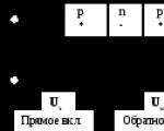
Semiconductor diodes
So, we figured out what a semiconductor is and what its operating principle is. Now let's move on to diodes, not the simplest radio-electronic elements. I already talked about the p-n junction above. Now in more detail: p is positive (positive), n is negative (negative, negative). Let's figure out how electrons move in a diode. Imagine if we connect a galvanic element, for example a battery, so that there is polarity. Oh yes - we didn’t understand the polarity. We already know the structure of the diode: p-n junction, p - positive is the anode, n - negative is the cathode. There is a thin white strip on the body of the diode - it is most often the cathode, it is connected to the minus, and the other terminal is the anode, which is connected to the plus. Now let's look at the movement of electrons. We have connected the polar leads of the diode, now a current arises. The electrons of the positive region begin to move towards the minus of the battery, and the electrons of the negative region begin to move towards the positive, they meet each other, the electrons seem to jump into holes, as a result, both ceased to exist. This electrical conductivity is called electron-hole electrical conductivity, electrons move with little resistance, shown in Figure 3 (A). This current is called direct current Ipr, but what happens if you change the polarity so that the anode is connected to the minus, and the cathode to the plus. What will happen? The positive area, in short, the holes will begin to move to the minus of the battery, and free electrons to the plus, as a result, a large area will appear, it is shaded in Figure 3 (B). This current is called reverse, which has a very high resistance, exceeding several hundred ohms, kilo-ohms and even mega-ohms.
So, we've sorted out the p-n junction, let's now talk about the purpose of the diode. Diodes are used for detector receivers to create pulsating direct current from alternating current. What is alternating current anyway? Let's remember. Alternating current is a current that is capable of changing its direction during each half-cycle, unit of time. How can a diode make alternating current pulsating? Here's how: you remember that a diode passes current only in one direction.

Figure 3. Movement of reverse and forward current electrons in a diode.
When the current begins to move from plus to minus, a forward current passes quietly without much resistance, but when the current begins to move from minus to plus, a reverse current arises, which the diode does not allow through. You've probably seen a graph of alternating voltage; such a wavy line is a sunusoid. If you cover the bottom line, you get a pulsating current. This means that the diode has cut off the lower part. The current will only move in one direction - from plus to minus. Got it? Then now let's move on to transistors.
Biopolar and field effect transistors
So, we come to biopolar and field-effect transistors. We will study only biopolar transistors, and we will not touch field-effect transistors for now - we will put them aside for the next lesson. Biopolar transistors are sometimes called simple transistors. In general, we have already studied semiconductors and their properties, as well as the diode and p-n junction. Now we come to a more complex structure. Structure? Do you think what it is, we have already studied the structure of the diode. Let us recall that the structure is several semiconductors having either hole conductivity or electronic conductivity; this structure is familiar as a p-n junction. A simple (bipolar) transistor has two structures. These are p-n-p structure and n-p-n structure. But you haven’t studied the findings. Well, of course, a simple transistor, like a field transistor, has three terminals. Only a regular transistor has a different name for the terminals and a different operating principle. Okay, let's look at the pnp structure. The first terminal is the base, which has a control current, the second terminal is the emitter, interacts with the base, and the third terminal is the collector, the increased current is removed from it. Now let’s determine where each output is and which area it belongs to. The first pin is the base, it belongs to the electronic region, that is, “n”, then the emitter belongs to the positive pin, which is to the left of the base, and the collector belongs to the positive pin, which is to the right of the base.
So, let's understand the principle of operation of the transistor. If the current is directed to the emitter and to the base, then you will get a p-n junction, there will be an excess of electrons, as a result, the collector will collect this strong flow of electrons and the current will be amplified. I forgot to say - a transistor, like a diode, can be in two states: closed and open. That's it, we have dealt with transistors and diodes, a drawing of two p-n-p and n-p-n structures is shown below.

Figure 4. Two transistor structures: p-n-p and n-p-n.
This article is finished, if something is not clear, please contact me, I will tell you and answer. Bye everyone. I was with you Dmitry Tsyvtsyn.
Discuss the article SEMICONDUCTOR TRANSISTORS AND DIODES