Semiconductor substances. Semiconductors - materials for preparing for the Unified State Exam in Physics
Along with conductors of electricity, there are many substances in nature that have significantly lower electrical conductivity than metal conductors. Substances of this kind are called semiconductors.
Semiconductors include: some chemical elements, such as selenium, silicon and germanium, sulfur compounds, such as thallium sulfide, cadmium sulfide, silver sulfide, carbides, such as carborundum,carbon (diamond),boron, gray tin, phosphorus, antimony, arsenic, tellurium, iodine and a number of compounds that include at least one of the elements of the 4th - 7th groups of the periodic system. There are also organic semiconductors.
The nature of the electrical conductivity of a semiconductor depends on the type of impurities present in the base material of the semiconductor and on the manufacturing technology of its components.
A semiconductor is a substance with 10 -10 - 10 4 (ohm x cm) -1, which, according to these properties, is between a conductor and an insulator. The difference between conductors, semiconductors and insulators according to band theory is as follows: in pure semiconductors and electronic insulators, there is an energy gap between the filled band (valence) and the conduction band.

Why do semiconductors conduct current?
A semiconductor has electronic conductivity if the outer electrons in its impurity atoms are relatively weakly bound to the nuclei of these atoms. If an electric field is created in a semiconductor of this kind, then, under the influence of the forces of this field, the outer electrons of the impurity atoms of the semiconductor will leave the confines of their atoms and turn into free electrons.
Free electrons will create an electric conduction current in the semiconductor under the influence of electric field forces. Consequently, the nature of the electric current in semiconductors with electronic conductivity is the same as in metal conductors. But since there are many times fewer free electrons in a unit volume of a semiconductor than in a unit volume of a metal conductor, it is natural that, under all other identical conditions, the current in a semiconductor will be many times less than in a metal conductor.
A semiconductor has “hole” conductivity if its impurity atoms not only do not give up their outer electrons, but, on the contrary, tend to capture electrons from the atoms of the main substance of the semiconductor. If an impurity atom takes an electron from an atom of the main substance, then in the latter something like a free space for an electron is formed - a “hole”.
A semiconductor atom that has lost an electron is called an “electron hole,” or simply a “hole.” If the “hole” is filled with an electron transferred from a neighboring atom, then it is eliminated and the atom becomes electrically neutral, and the “hole” is displaced to the neighboring atom that has lost the electron. Consequently, if a semiconductor with “hole” conductivity is exposed to an electric field, then the “electron holes” will shift in the direction of this field.
Bias "electron holes" in the direction of the electric field is similar to the movement of positive electric charges in the field and therefore represents the phenomenon of electric current in a semiconductor.
Semiconductors cannot be strictly distinguished by the mechanism of their electrical conductivity, since, along withWith “hole” conductivity, a given semiconductor may, to one degree or another, also have electronic conductivity.
Semiconductors are characterized by:
type of conductivity (electronic - n-type, hole - p-type);
resistivity;
lifetime of charge carriers (minority) or diffusion length, surface recombination rate;
dislocation density.
Silicon is the most common semiconductor material
Temperature has a significant influence on the characteristics of semiconductors. An increase in it predominantly leads to a decrease in resistivity and vice versa, i.e. semiconductors are characterized by the presence of a negative . Near absolute zero, a semiconductor becomes an insulator.
Semiconductors are the basis of many devices. In most cases they must be obtained in the form of single crystals. To impart specified properties, semiconductors are doped with various impurities. Increased demands are placed on the purity of source semiconductor materials.

Semiconductors have found the widest application in modern technology; they have had a very strong influence on technical progress. Thanks to them, it is possible to significantly reduce the weight and dimensions of electronic devices. The development of all areas of electronics leads to the creation and improvement of a large number of various equipment based on semiconductor devices. Semiconductor devices serve as the basis for microcells, micromodules, solid-state circuits, etc.
Electronic devices based on semiconductor devices are practically inertia-free. A carefully constructed and well-sealed semiconductor device can last tens of thousands of hours. However, some semiconductor materials have a low temperature limit (for example, germanium), but not very complex temperature compensation or replacing the main material of the device with another (for example, silicon, silicon carbide) largely eliminates this disadvantage. Improving the technology of manufacturing semiconductor devices leads to a reduction in the existing scatter and instability of parameters.

The semiconductor-metal contact and electron-hole junction (n-p junction) created in semiconductors are used in the manufacture of semiconductor diodes. Double junctions (p-n-p or n-p-n) - transistors and thyristors. These devices are mainly used for rectifying, generating and amplifying electrical signals.
Based on the photoelectric properties of semiconductors, photoresistors, photodiodes and phototransistors are created. The semiconductor serves as the active part of oscillation generators (amplifiers). When electric current is passed through a pn junction in the forward direction, charge carriers - electrons and holes - recombine with the emission of photons, which is used to create LEDs.

The thermoelectric properties of semiconductors made it possible to create semiconductor thermal resistances, semiconductor thermoelements, thermopiles and thermoelectric generators, and thermoelectric cooling of semiconductors, based on the Peltier effect, - thermoelectric refrigerators and thermostabilizers.
Semiconductors are used in machineless converters of thermal and solar energy into electricity - thermoelectric generators, and photoelectric converters (solar batteries).
Mechanical stress applied to a semiconductor changes its electrical resistance (the effect is stronger than in metals), which was the basis of the semiconductor strain gauge.
Semiconductor devices have become widespread in world practice, revolutionizing electronics; they serve as the basis for the development and production of:
measuring equipment, computers,
equipment for all types of communications and transport,
for process automation in industry,
devices for scientific research,
rocket technology,
medical equipment
other electronic devices and instruments.
The use of semiconductor devices makes it possible to create new equipment and improve old ones, which means a reduction in its dimensions, weight, power consumption, and therefore a decrease in heat generation in the circuit, an increase in strength, immediate readiness for action, and can increase the service life and reliability of electronic devices. devices.
Historical information
Semiconductors, as a special class of substances, have been known since the end of the 19th century, only the development of solid state theory made it possible to understand their features long before they were discovered:
1. effect of current rectification at the metal-semiconductor contact
2. photoconductivity.
The first devices based on them were built.
O. V. Losev (1923) proved the possibility of using semiconductor-metal contacts to amplify and generate oscillations (crystal detector). However, in subsequent years, crystal detectors were supplanted by electron tubes, and only in the early 50s, with the discovery of transistors (USA 1949), did the widespread use of semiconductors (mainly germanium and silicon in radio electronics) begin. At the same time, intensive study of the properties of semiconductors began, which was facilitated by the improvement of methods cleaning crystals and doping them (introducing certain impurities into the semiconductor).
In the USSR, the study of semiconductors began in the late 20s under the leadership of A.F. Ioffe at the Physico-Technical Institute of the USSR Academy of Sciences.
Interest in the optical properties of semiconductors has increased due to the discovery of stimulated emission in semiconductors, which led to the creation of semiconductor lasers, first on the p-n junction, and then on heterojunctions.
Recently, devices based on the action of semiconductors have become more widespread. These substances began to be studied relatively recently, but neither modern electronics, nor medicine, nor many other sciences can do without them.
Properties of semiconductors
Semiconductors- a wide class of substances, characterized by values of specific electrical conductivity d, lying in the range between the specific electrical conductivity of metals and good dielectrics, that is, these substances cannot be classified as either dielectrics (since they are not good insulators) or metals (they are not good conductors of electric current). Semiconductors, for example, include substances such as germanium, silicon, selenium, tellurium, as well as some oxides, sulfides and alloys of metals.
Semiconductors have not attracted much attention from scientists and engineers for a long time. One of the first to begin systematic research into the physical properties of semiconductors was the outstanding Soviet physicist Abram Fedorovich Ioffe. He found out that semiconductors are a special class of crystals with many remarkable properties:
1) With increasing temperature, the resistivity of semiconductors decreases, in contrast to metals, whose resistivity increases with increasing temperature. Moreover, as a rule, over a wide temperature range, this increase occurs exponentially:
d = dо ∙ exp. (-ea/kT)
where ea is the so-called conduction activation energy,
dо - coefficient depending on temperature
The resistivity of semiconductor crystals may also decrease when exposed to light or strong electronic fields.
2) The property of one-way conductivity of the contact of two semiconductors. It is this property that is used in the creation of various semiconductor devices: diodes, transistors, thyristors, etc.
3) Contacts of various semiconductors under certain conditions when illuminated or heated are sources of photo-e. d.s. or, accordingly, thermo-e. d.s.
The structure of semiconductors and the principle of their operation.
As already mentioned, semiconductors are a special class of crystals. Valence electrons form regular covalent bonds, shown schematically in Fig. 1. Such an ideal semiconductor does not conduct electric current at all (in the absence of lighting and radiation exposure).
Just as in nonconductors, electrons in semiconductors are bonded to atoms, but this bond is very weak. As the temperature rises
(T>0 K), under illumination or irradiation, electronic bonds can be broken, which will lead to the separation of an electron from the atom (Fig. 2). Such an electron is a current carrier. The higher the temperature of the semiconductor, the higher the concentration of conduction electrons, therefore, the lower the resistivity. Thus, the decrease in the resistance of semiconductors when heated is due to an increase in the concentration of current carriers in it.
Unlike conductors, current carriers in semiconductor substances can be not only electrons, but also “holes.” When one of the semiconductor atoms loses an electron, an empty space remains in its orbit - a “hole”; when an electric field is applied to the crystal, the “hole” as a positive charge moves towards vector E, which actually occurs due to the breaking of some bonds and the restoration of others. A “hole” can conventionally be considered a particle carrying a positive charge.
Impurity conductivity .
The same semiconductor has either electronic,or hole conductivity - this depends on the chemical composition of the introduced impurities. Impurities have a strong effect on the electrical conductivity of semiconductors:
for example, thousandths of a percent of impurities can be hundreds of thousands of times
reduce their resistance. This fact, on the one hand, indicates the possibility of changing the properties of semiconductors; on the other hand, it indicates the difficulties of technology in the manufacture of semiconductor materials with given characteristics.
When considering the mechanism of the influence of impurities on the electrical conductivity of semiconductors, two cases should be considered:
Electronic conductivity .
Adding electron-rich impurities to germanium, such as arsenic or antimony, makes it possible to obtain a semiconductor with electronic conductivity or n-type semiconductor (from the Latin word “negativus” - “negative”).
In Fig. Figure 3a schematically shows the picture of electron bonds at 0 K. One of the valence electrons of arsenic does not participate in bonds with other atoms. As the temperature increases, an electron can be torn away from the atom (see Fig. 3b) and thereby creates electronic conductivity.
Impurities that create such electrical conductivity are called donors.
Hole conductivity
The addition of aluminum, gallium or indium to the same germanium creates an excess of holes in the crystal. Then the semiconductor will have hole conductivity - p-type semiconductor.
Hole impurity electrical conductivity is created by atoms having fewer valence electrons than the main atoms. In Fig. Figure 4 schematically shows the electronic connections of germanium with a boron impurity. At 0 K, all bonds are complete, only boron lacks one bond (see Fig. 4a). However, with increasing temperature, boron can saturate its bonds at the expense of electrons from neighboring atoms (see Fig. 4b).
Such impurities are called acceptor impurities.
Liquid semiconductors
The melting of many crystalline semiconductors is accompanied by a sharp increase in their electrical conductivity Q to values typical for metals (see Fig. 5a). However, a number of semiconductors (for example, HgSe, HgTe, etc.) are characterized by the preservation or decrease of Q during melting and the semiconductors retain the nature of the temperature dependence of Q (see Fig. 5b). Some liquid semiconductors, with a further increase in temperature, lose their semiconducting properties and acquire metallic properties (for example, Te - Se alloys, and Te alloys). Te - Se alloys rich in Se behave differently; their electrical conductivity is purely semiconductor in nature.
In liquid semiconductors, the role of the band gap is played by the energy region near the minimum density of states in the energy spectrum of electrons.
If the minimum is sufficiently deep, a zone of almost localized states of charge carriers with low mobility (pseudogap) appears in its vicinity. If the pseudogaps “collapse” as the temperature increases, the liquid semiconductor turns into a metal.
Use of semiconductors.
The most important semiconductor devices for technology - diodes, transistors, thyristors are based on the use of remarkable materials with electronic or hole conductivity.
The widespread use of semiconductors began relatively recently, and now they have become very widely used. They convert light and thermal energy into electrical energy and, conversely, create heat and cold using electricity. Semiconductor devices can be found in a conventional radio receiver and in a quantum generator - a laser, in a tiny atomic battery and in microprocessors.
Engineers cannot do without semiconductor rectifiers,
switches and amplifiers. Replacing tube equipment with semiconductor equipment has made it possible to reduce the size and weight of electronic devices tenfold, reduce their power consumption and dramatically increase reliability.
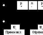
Semiconductors are widely used in technology. The action of a semiconductor diode is based on different conductivity (p- and n-type). When semiconductors with p- and n-conductivity come into contact with a certain direction of current, a barrier layer is created in the circuit (Fig. 19.4) - a double electric layer, the field of which prevents the transfer of charge carriers. This is the basis of the action of the semiconductor diode, which serves to rectify alternating current. Selenium rectifiers were among the first to become widespread.
In addition to diodes, semiconductor triodes are also widely used in radio engineering - transistors in which there are two p-n junctions: either p-n-p or n-p-n.
The strong temperature dependence of semiconductors is used in thermistors, highly sensitive devices for measuring temperature.
Among the many applications of semiconductors is also solar cells, the operation of which is based on the photoconductivity of semiconductors - the ability to change resistance under the influence of light (a phenomenon similar to the photoelectric effect, which occurs entirely within a solid matter).
Magnetic forces
The magnetic properties of substances have been known since ancient times. Described by ancient scientists as a stone that attracts iron, it is a natural magnet - a mineral that is quite often found in nature. It consists of iron compounds (FeO - 31% and Fe 2 O 3 - 69%). Already in 1600, V. Gilbert’s work “On the Magnet, Magnetic Bodies and the Great Magnet of the Earth” was published, which contained a generalization of a large number of experimental facts. The main ones were as follows:
1) a magnet has two poles - north and south, different in their properties,
2) unlike poles attract, like poles repel;
3) the magnetic needle is located in space in a certain way, pointing north to south;
4) it is impossible to obtain a magnet with one pole;
5) The earth is a big magnet.
The nature of magnetic phenomena was revealed only after the experimental facts were established in the 19th century that electric current (moving charges) create a magnetic field (R. Erstad, 1820). The study of the interaction of conductors with currents, as a result of which it was found that parallel currents of the same direction are attracted , and the opposite ones repel (J.Amper, I820), led to the conclusion that the forces of interaction between moving electric charges differ from the forces of interaction between stationary charges.
Additional forces arising between moving charges are called magnetic forces. This is due to the fact that they were discovered by the effect of current on a magnetic needle.
Thus, all magnetic disturbances can be reduced to electric ones, and magnetic forces, as Einstein showed, are a relativistic correction to Coulomb’s law.
While there is no current in the conductors, no interaction forces arise between them, because the positive charge of the ions of the metal crystal lattice and the negative charge of the electrons are distributed evenly and the total charge inside the conductor is zero. In the presence of current, due to the movement of electrons, the average distance between them is reduced by a factor, where
V is the drift velocity of electrons. As a result, the electron charge density will increase by a factor of two and, therefore, the resulting charge will not be zero. This leads to the interaction of conductors.
One of the main properties of a p‑n‑junction is its ability to pass electric current in one (forward) direction thousands and millions of times better than in the reverse direction.
Semiconductors are a class of substances that occupy an intermediate position between substances that conduct electric current well (conductors, mainly metals) and substances that practically do not conduct electric current (insulators or dielectrics).
Semiconductors are characterized by a strong dependence of their properties and characteristics on the microscopic amounts of impurities they contain. By changing the amount of impurity in a semiconductor from ten millionths of a percent to 0.1–1%, you can change their conductivity by millions of times. Another important property of semiconductors is that electric current is carried into them not only by negative charges - electrons, but also by positive charges of equal magnitude - holes.
If we consider an idealized semiconductor crystal, absolutely free of any impurities, then its ability to conduct electric current will be determined by the so-called intrinsic electrical conductivity.
Atoms in a semiconductor crystal are connected to each other using electrons in the outer electron shell. During thermal vibrations of atoms, thermal energy is distributed unevenly between the electrons forming bonds. Individual electrons can receive enough thermal energy to “break away” from their atom and be able to move freely in the crystal, i.e., become potential current carriers (in other words, they move into the conduction band). Such electron departure violates the electrical neutrality of the atom; it acquires a positive charge equal in magnitude to the charge of the departed electron. This vacant space is called a hole.
Since the vacant place can be occupied by an electron from a neighboring bond, the hole can also move inside the crystal and become a positive current carrier. Naturally, under these conditions, electrons and holes appear in equal quantities, and the electrical conductivity of such an ideal crystal will be equally determined by both positive and negative charges.
If in place of an atom of the main semiconductor we place an impurity atom, the outer electron shell of which contains one more electron than the atom of the main semiconductor, then such an electron will turn out to be superfluous, unnecessary for the formation of interatomic bonds in the crystal and weakly connected with its atom. Tens of times less energy is enough to tear it away from its atom and turn it into a free electron. Such impurities are called donor, i.e., donating an “extra” electron. The impurity atom is charged, of course, positively, but no hole appears, since a hole can only be an electron vacancy in an unfilled interatomic bond, and in this case all bonds are filled. This positive charge remains associated with its atom, motionless and, therefore, cannot take part in the process of electrical conductivity.
The introduction of impurities into a semiconductor, the outer electron shell of which contains fewer electrons than in the atoms of the main substance, leads to the appearance of unfilled bonds, i.e. holes. As mentioned above, this vacancy can be occupied by an electron from a neighboring bond, and the hole is able to move freely throughout the crystal. In other words, the movement of a hole is a sequential transition of electrons from one neighboring bond to another. Such impurities that “accept” an electron are called acceptor impurities.

If a voltage (as indicated in the polarity diagram) is applied to the metal-dielectric semiconductor structure of the n-type, then an electric field arises in the near-surface layer of the semiconductor, repelling electrons. This layer turns out to be depleted.

In a p-type semiconductor, where the majority carriers are positive charges - holes, the polarity of the voltage that repelled electrons will attract holes and create an enriched layer with reduced resistance. A change in polarity in this case will lead to repulsion of holes and the formation of a near-surface layer with increased resistance.
With an increase in the amount of impurities of one type or another, the electrical conductivity of the crystal begins to acquire an increasingly pronounced electronic or hole character. In accordance with the first letters of the Latin words negativus and positivus, electronic electrical conductivity is called n-type electrical conductivity, and hole conductivity is called p-type, indicating which type of mobile charge carriers for a given semiconductor is the main one and which is the minor one.
With electrical conductivity due to the presence of impurities (i.e., impurity), there are still 2 types of carriers left in the crystal: the main ones, which appear mainly due to the introduction of impurities into the semiconductor, and the minority ones, which owe their appearance to thermal excitation. The content in 1 cm 3 (concentration) of electrons n and holes p for a given semiconductor at a given temperature is a constant value: n − p = const. This means that, by increasing the concentration of carriers of a given type by several times due to the introduction of impurities, we reduce the concentration of carriers of another type by the same amount. The next important property of semiconductors is their strong sensitivity to temperature and radiation. As the temperature rises, the average vibration energy of the atoms in the crystal increases, and more and more bonds will be broken. More and more pairs of electrons and holes will appear. At sufficiently high temperatures, the intrinsic (thermal) conductivity can be equal to the impurity conductivity or even significantly exceed it. The higher the concentration of impurities, the higher the temperatures this effect will occur.
Bonds can also be broken by irradiating the semiconductor, for example, with light, if the energy of light quanta is sufficient to break the bonds. The energy of breaking bonds is different for different semiconductors, so they react differently to certain parts of the irradiation spectrum.
Silicon and germanium crystals are used as the main semiconductor materials, and boron, phosphorus, indium, arsenic, antimony and many other elements that impart the necessary properties to semiconductors are used as impurities. The production of semiconductor crystals with a given impurity content is a complex technological process, carried out in especially clean conditions using equipment of high precision and complexity.
All of the listed most important properties of semiconductors are used to create semiconductor devices that are very diverse in their purposes and areas of application. Diodes, transistors, thyristors and many other semiconductor devices are widely used in technology. The use of semiconductors began relatively recently, and today it is difficult to list all their “professions.” They convert light and thermal energy into electrical energy and, conversely, create heat and cold using electricity (see Solar energy). Semiconductor devices can be found in a conventional radio receiver and in a quantum generator - a laser, in a tiny atomic battery and in miniature blocks of an electronic computer. Engineers today cannot do without semiconductor rectifiers, switches and amplifiers. Replacing tube equipment with semiconductor equipment has made it possible to reduce the size and weight of electronic devices tenfold, reduce their power consumption and dramatically increase reliability.
You can read about this in the article Microelectronics.
There is nothing extraordinarily important or interesting in this article, just an answer to a simple question for “dummies”: what are the main properties that distinguish semiconductors from metals and dielectrics?
Semiconductors are materials (crystals, polycrystalline and amorphous materials, elements or compounds) with the existence of a band gap (between the conduction band and the valence band).
Electronic semiconductors are crystals and amorphous substances that, in terms of electrical conductivity, occupy an intermediate position between metals (σ = 10 4 ÷10 6 Ohm -1 cm -1) and dielectrics (σ = 10 -10 ÷10 -20 Ohm -1 cm -1). However, the given boundary values of conductivity are very arbitrary.
Band theory makes it possible to formulate a criterion that makes it possible to divide solids into two classes - metals and semiconductors (insulators). Metals are characterized by the presence of free levels in the valence band, to which electrons can move, receiving additional energy, for example, due to acceleration in an electric field. A distinctive feature of metals is that in their ground, unexcited state (at 0 K) they have conduction electrons, i.e. electrons that participate in ordered movement under the influence of an external electric field.
In semiconductors and insulators at 0 K, the valence band is completely populated, and the conduction band is separated from it by a band gap and does not contain carriers. Therefore, a not too strong electric field is not able to strengthen the electrons located in the valence band and transfer them to the conduction band. In other words, such crystals at 0 K should be ideal insulators. When the temperature increases or such a crystal is irradiated, electrons can absorb quanta of thermal or radiant energy sufficient to move into the conduction band. During this transition, holes appear in the valence band, which can also participate in the transfer of electricity. The probability of an electron transferring from the valence band to the conduction band is proportional to ( -Eg/ kT), Where Eg - width of the forbidden zone. With a large value Eg (2-3 eV) this probability turns out to be very small.
Thus, the division of substances into metals and non-metals has a very definite basis. In contrast, the division of nonmetals into semiconductors and dielectrics does not have such a basis and is purely conditional.
Previously, it was believed that substances with a band gap could be classified as dielectrics Eg≈ 2÷3 eV, but later it turned out that many of them are typical semiconductors. Moreover, it was shown that, depending on the concentration of impurities or excess (above the stoichiometric composition) atoms of one of the components, the same crystal can be both a semiconductor and an insulator. This applies, for example, to crystals of diamond, zinc oxide, gallium nitride, etc. Even such typical dielectrics as barium and strontium titanates, as well as rutile, upon partial reduction, acquire the properties of semiconductors, which is associated with the appearance of excess metal atoms in them.
The division of nonmetals into semiconductors and dielectrics also has a certain meaning, since a number of crystals are known whose electronic conductivity cannot be noticeably increased either by introducing impurities or by illumination or heating. This is due either to the very short lifetime of photoelectrons, or to the existence of deep traps in crystals, or to the very low mobility of electrons, i.e. with an extremely low speed of their drift in an electric field.
Electrical conductivity is proportional to the concentration n, the charge e and the mobility of charge carriers. Therefore, the temperature dependence of the conductivity of various materials is determined by the temperature dependences of the indicated parameters. For all electronic conductors charge e constant and independent of temperature. In most materials, the mobility value usually decreases slightly with increasing temperature due to an increase in the intensity of collisions between moving electrons and phonons, i.e. due to electron scattering by vibrations of the crystal lattice. Therefore, the different behavior of metals, semiconductors and dielectrics is mainly associated with the charge carrier concentration and its temperature dependence:
1) in metals, the concentration of charge carriers n is high and changes slightly with temperature changes. The variable included in the equation for electrical conductivity is mobility. And since mobility slightly decreases with temperature, electrical conductivity also decreases;
2) in semiconductors and dielectrics n usually increases exponentially with temperature. This rapid growth n makes the most significant contribution to changes in conductivity than a decrease in mobility. Therefore, electrical conductivity increases rapidly with increasing temperature. In this sense, dielectrics can be considered as a certain limiting case, since at ordinary temperatures the value n in these substances is extremely small. At high temperatures, the conductivity of individual dielectrics reaches the semiconductor level due to an increase n. The opposite is also observed - at low temperatures, some semiconductors become insulators.
Bibliography
- West A. Chemistry of solids. Part 2 Per. from English - M.: Mir, 1988. - 336 p.
- Modern crystallography. T.4. Physical properties of crystals. - M.: Nauka, 1981.
Students of group 501 of the Faculty of Chemistry: Bezzubov S.I., Vorobyova N.A., Efimov A.A.